
The device you’re reading this article on is a very complex piece of technology. Being a smartphone, a computer, a tablet, or anything else you can browse the internet with, it’s “brain” is the CPU, the central processing unit, where the core calculations take place. The technology behind CPUs was a main conductor of the Third Industrial Revolution, promoting economic and social development in never-before-seen proportions.
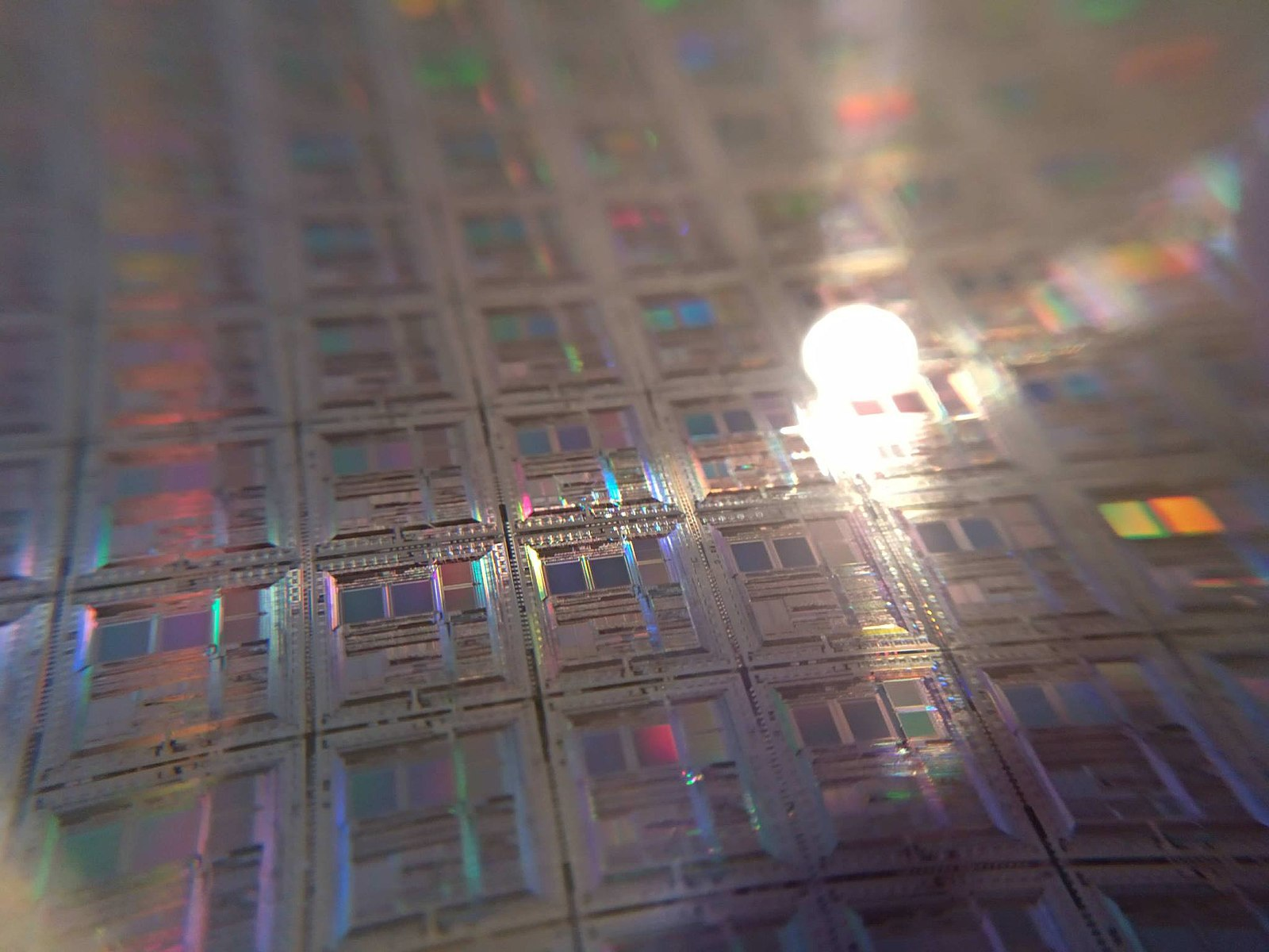
Photo by Le hollandais volant. This file is licensed under the Creative Commons Attribution 4.0 International license.
CPU manufacturing
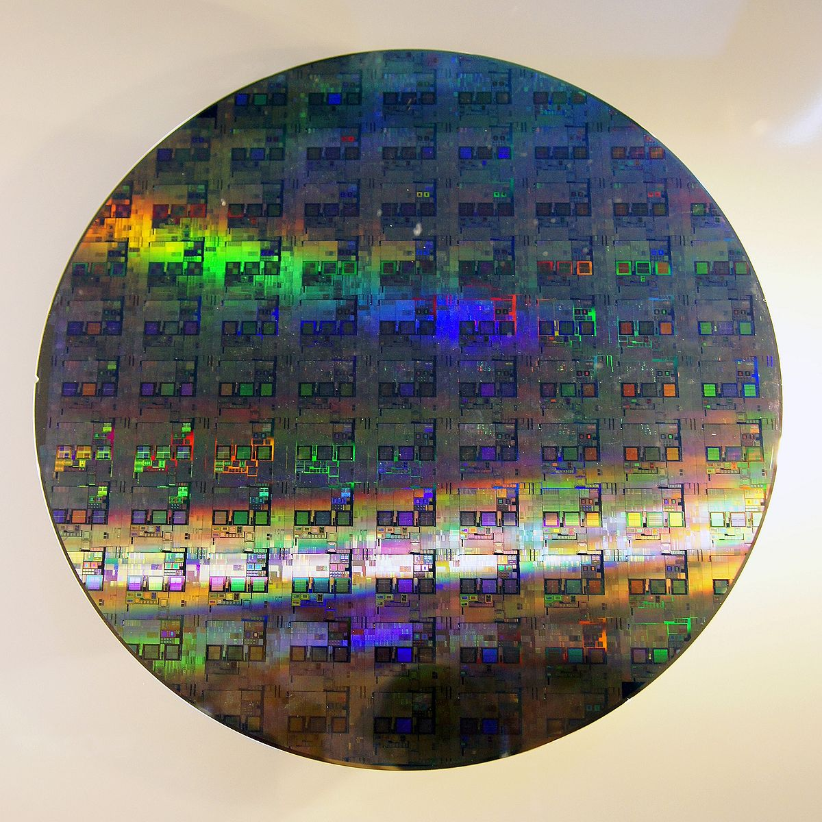
Processors are built on silicon wafers, which are thin slices of extremely pure silicon. As it’s circuit components are extremely small (in the order of hundreds of atoms), a single atom in the wrong place can ruin an entire chip. For that reason, at least 99.9999999% of the atoms in the slice must be silicon atoms, or, in other words, at most 1 out of every billion atoms may not be a silicon atom.
Designing
Processors are electric circuits, just as the one that lights your home. The difference is that a processor is analogous to a house with hundreds of billions of individual light bulbs, which is in the order of all light bulbs in the world. And they all have to work.
The companies that design the circuits (such as Apple, Intel, AMD and Samsung) use high-end proprietary software to blueprint the circuit’s “maps” and test them. It’s impossible to design a modern CPU without using a modern CPU!
Once completed, the circuit design is sent to a “semiconductor fabrication plant”, the place where it’s “printed”.
Who wants a sand wafer? ?
It all starts with sand. Well… Not quite sand, but high purity quartzite, which is a kind of rock. Both sand and quartzite are composed mostly of atoms of oxygen and silicon, but quartzite is much purer. Sand is usually “dirty”, that is, contaminated with many other kinds of atoms we would have to get rid of. It’s theoretically possible to use sand instead of quartzite, but it would be way more expensive.
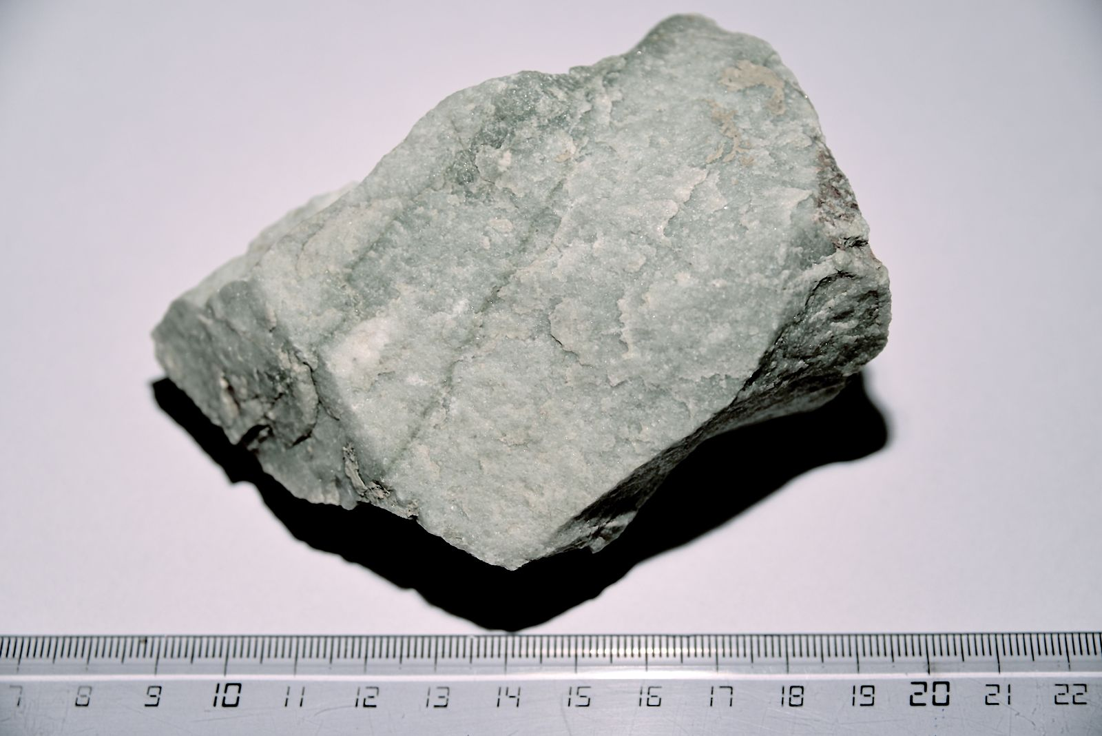
Sample of quartzite extracted from Maurienne Valley in the French Alps
Photo by Gabriel Haute Maurienne. This file is licensed under the Creative Commons Attribution-Share Alike 4.0 International license.
Quartzite is then mixed with coal and melted in furnaces at temperatures in the order of 2000°C to get rid of the oxygen atoms. That process yields metallurgical grade silicon, which is 98% to 99% pure.
Metallurgical silicon is further purified though very energy-intensive chemical reactions and separation methods to get electronic grade silicon.
Electronic grade silicon is then melted again at very high temperatures and solidified very slowly under strictly controlled conditions to make sure all of the silicon atoms get perfectly aligned. We end up with a huge cylinder of amazingly pure silicon.

Silicon ingot, an almost pure silicon cylinder
Photo by Stahlkocher. This file is licensed under the Creative Commons Attribution-Share Alike 3.0 Unported license.
Each one of these big cylinders is further cut in many slices, the silicon wafers, which are usually 30cm wide and 0.8mm thin.
Once the silicon wafers are polished, they must be handled extremely carefully, in atmospheres way cleaner than an operating room, to avoid contamination.
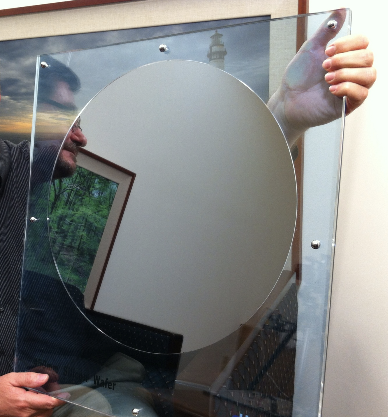
Silicon wafer
Photo by Intel Free Press. Cropped. This file is licensed under the Creative Commons Attribution 2.0 Generic license.
Photolithography
Once we have our polished, beautiful, pure, expensive and shiny silicon wafer, the actual circuit must be “printed” on it. That is done using an extremely precise machine which is about the size of a school bus, with hundreds of thousands of parts and weighing hundreds of tons. Just to give a sense of the mechanical complexity of these machines, it has parts that weigh around 200kg and accelerate faster than a fighter jet.
First, the wafer is “cooked” at 1000°C to create an oxidized film on top of it. Subsequently, it gets covered with a special material that is degraded by light.
After that, the machine uses ultraviolet radiation and a set of special lenses and mirrors to transfer the circuit “map” to the wafer while shrinking it to a ridiculously small scale. The degraded parts of the material are “washed away”, leaving the wafer with a nanometric maze stencil.
The wafer is then treated with special materials to form a layer on top of it’s unprotected parts, in analogy of a spray paint stencil.
This process of “painting” is repeated a series of times to form the many layers of the chips, which are then tested and scanned by electron microscopes to make sure each single connection of the nanometric circuit works properly.
Depending on their size, several dozen or several hundred processors can be fabricated on one wafer, but, as it’s impossible to completely get rid of impurities, ordinarily some of the chips have to be thrown away. As was said, a few atoms out of place can prevent a whole CPU from working.
Finally, the wafers get sliced and each individual chip is ready to be soldered to its container and be further tested, packaged and assembled with the other components that make your device, such as the motherboard and storage devices. Buon appetito!
Silicon wafer ready to be cut into single chips
Photo by Peellden. This file is licensed under the Creative Commons Attribution-Share Alike 3.0 Unported license.